Microstructure Analysis (SEM-EDS)
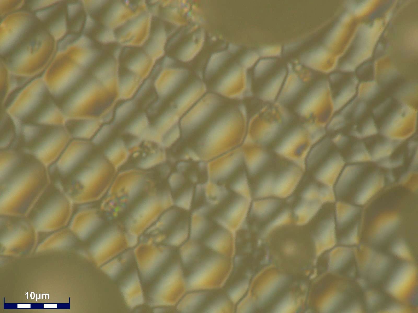
Microstructure analysis is the study of a material’s internal structure at the microscopic level to evaluate its properties, performance, and potential failure mechanisms. Through careful sample preparation including sectioning, mounting, polishing, and etching, we reveal features such as grain size, phase distribution, inclusions, porosity, and microstructural defects. Using high-resolution optical and 3D microscopy as well as scanning electron microscopy (SEM) with energy-dispersive spectroscopy (EDS), we can characterize complex phases, quantify microconstituents, and assess the effects of heat treatment or processing. This detailed examination provides critical insight into mechanical behavior, material consistency, and root causes of failure, supporting engineers and quality professionals in making informed decisions.
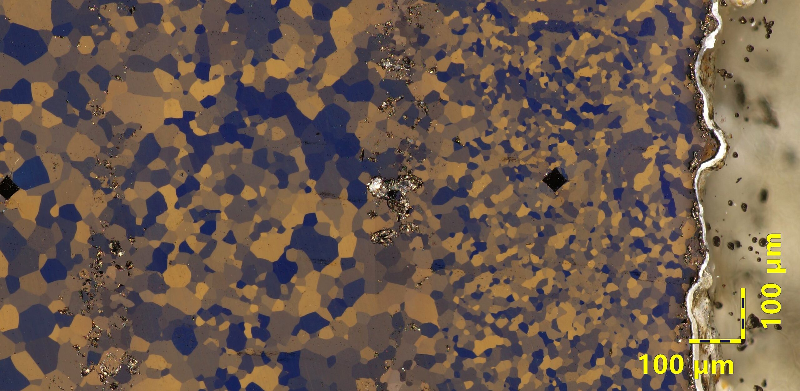
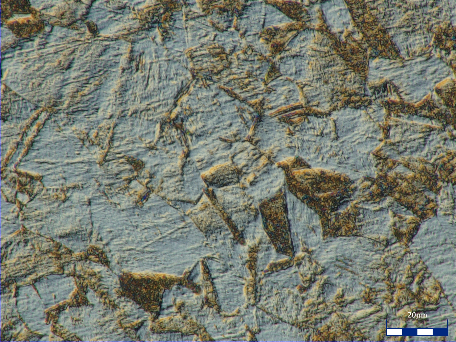
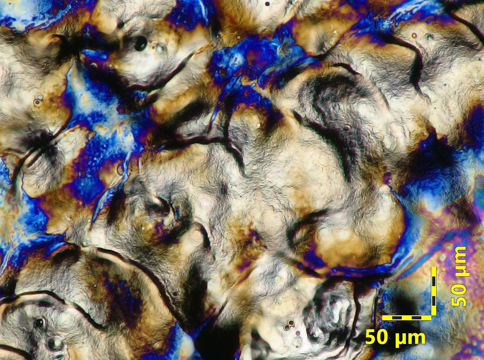
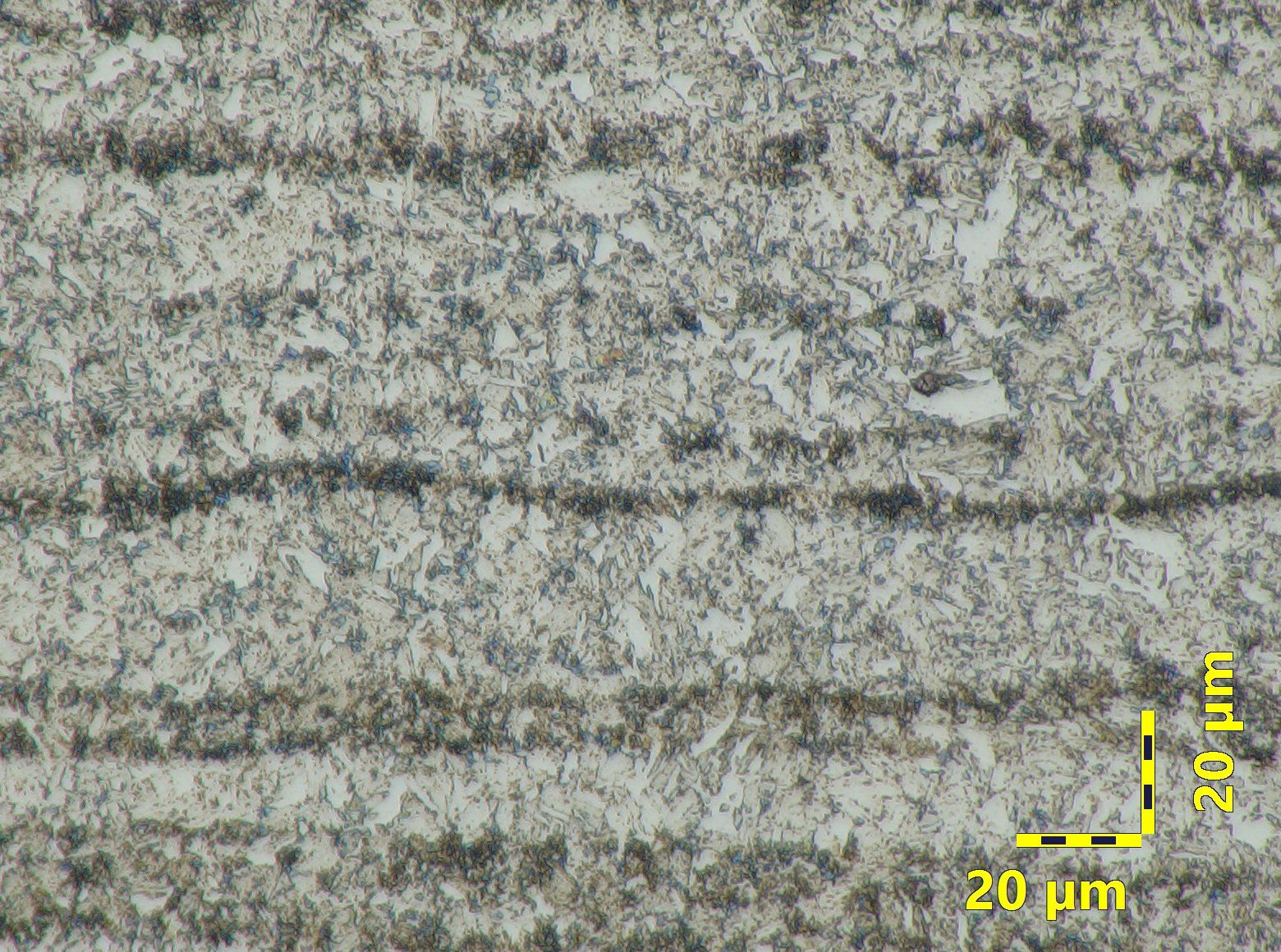
Microstructure is the internal arrangement of grains, phases, and inclusions within a material, and it plays a key role in determining strength, toughness, and overall performance. In metals and alloys formed from a melt, factors such as cooling rate, section thickness, and solidification conditions control grain size, shape, and phase distribution. Subsequent processing, including hot or cold working and heat treatment, can refine the structure and modify phase content. In powder-processed materials, particle characteristics and sintering history largely determine the final microstructure. Alloying elements, impurities, and additives further influence phase stability, carbide networks, and graphite formation. Microstructure may also evolve during service due to thermal exposure, mechanical stress, or corrosion. Careful analysis and control of these features are essential for predicting material behavior, ensuring quality, and preventing failure.
At PMI specialists, we use a combination of techniques including optical and Scanning Electron Microscopy (SEM) and Energy Dispersive Spectroscopy (EDS) to determine the microstructures and chemical analysis on a variety of materials. Our wealth of expertise in materials including alloys, polymers, ceramics and composites can be accessed to solve problems with typical applications including:
- Grain size/grain flow
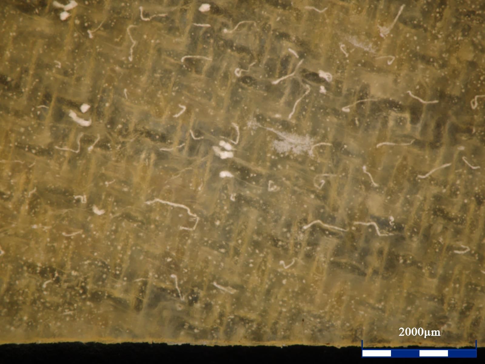
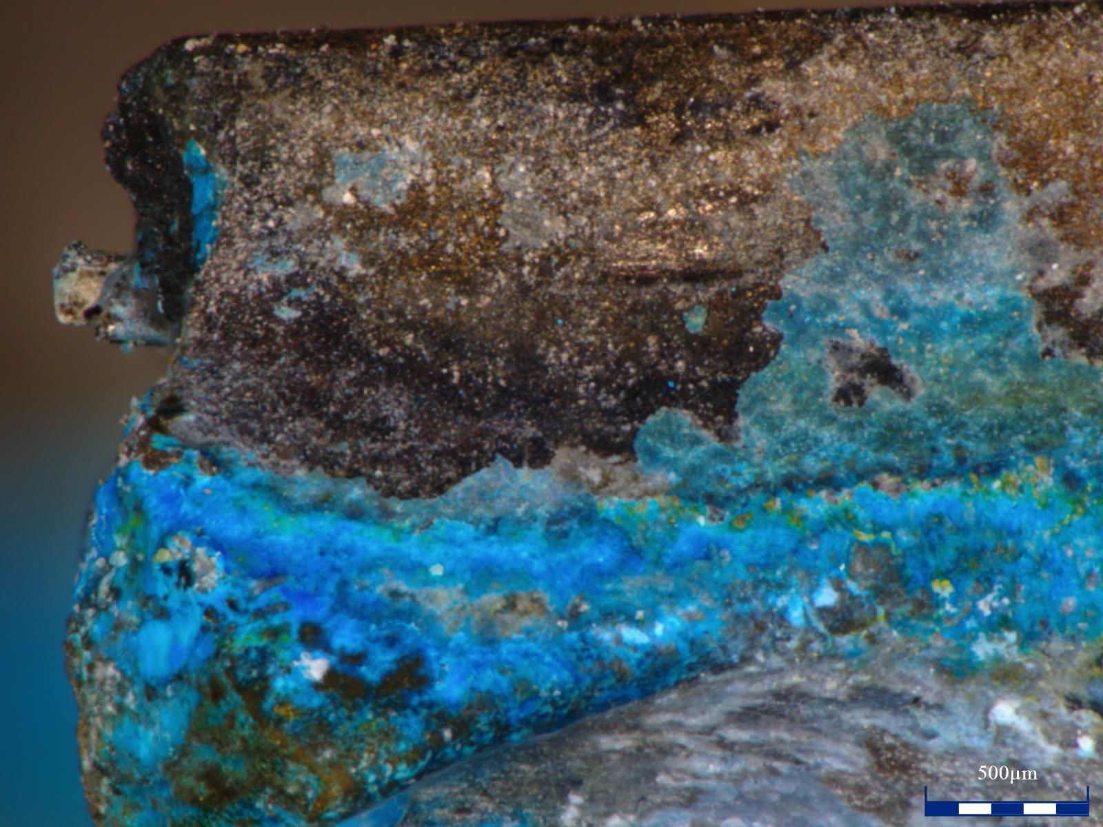
- Identification of inclusions and specks
- Porosity and bonding evaluation
- Refractory attack mechanisms
- Fiber/matrix debonding
- Surface deposits and coatings
- Development of interfaces on reaction
- Unknown particles or materials identification
- Evaluation of material processing
- Performance evaluation and variability
- Failure mechanisms and crack development
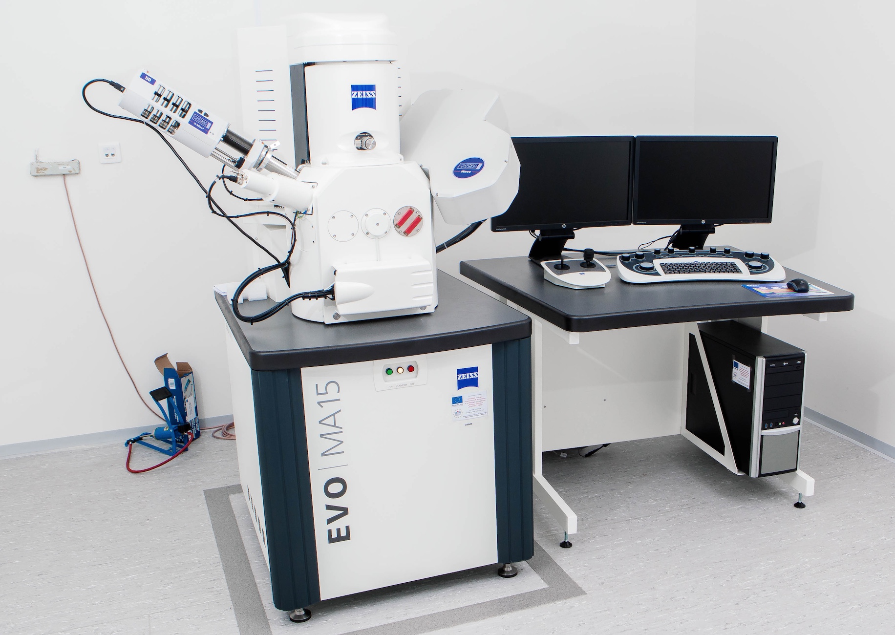
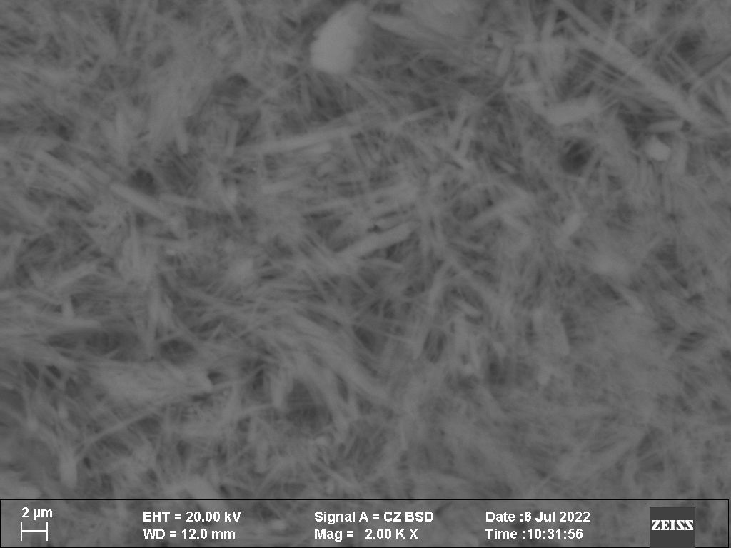
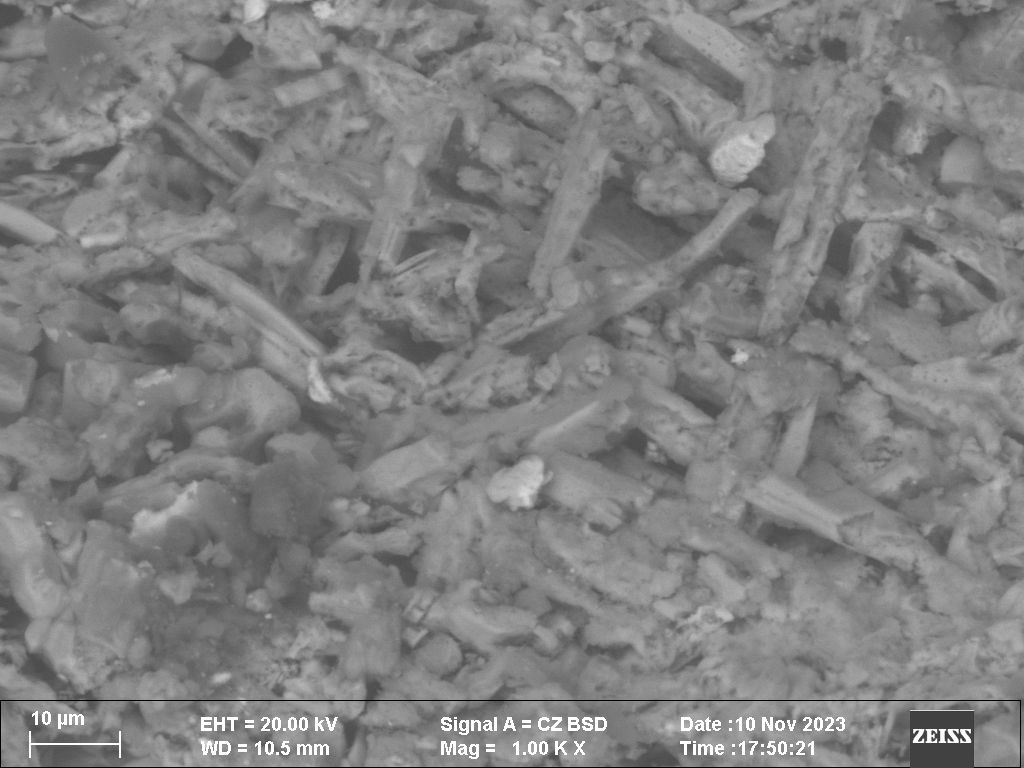
Our new variable pressure Zeiss EVO MA-15 SEM is equipped with a newly developed third generation variable pressure secondary electron detector, which allows high resolution microstructure imaging possible on non-conductive, wet or volatile samples. Typical samples we can handle include corrosion products, cloth, polymer films, plastic components, printed-circuit boards, ceramics, rocks, painted and coated metals, explanted medical devices with attached tissue, metal components encapsulated in polymer, lubricated metals and polymers. In many of these cases, evaporative or sputter coating was either undesirable or not possible. These examples show the value of eliminating sample pretreatment and the utility for performing scanning electron microscopy at variable pressures.
Pricing $325 per hour.