SEM-EDS
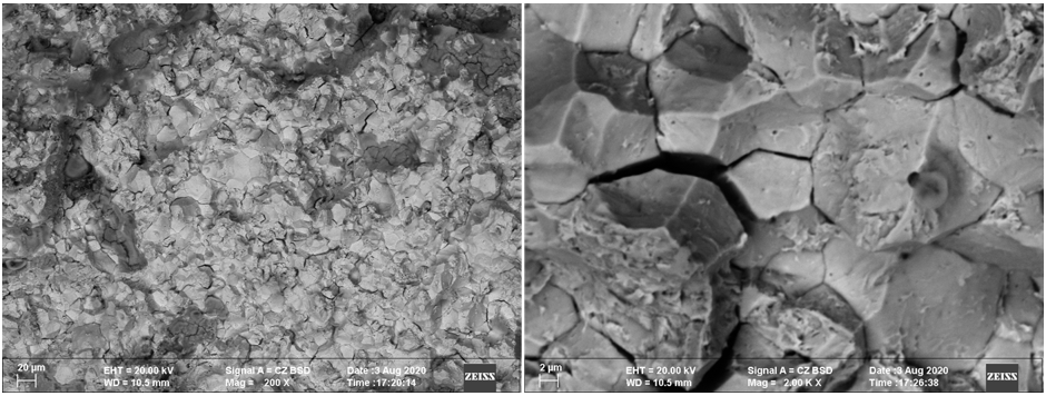
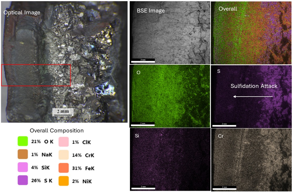
Scanning Electron Microscopy (SEM) combined with Energy Dispersive Spectroscopy (EDS) provides powerful insight into the microstructure, fracture behavior, and chemical composition of materials. Our metallurgical lab delivers high-resolution imaging and precise elemental analysis to support failure investigations, corrosion studies, and materials verification.
What SEM/EDS Can Do For you:
- Identify fracture modes (ductile, brittle, fatigue, SCC, hydrogen-related)
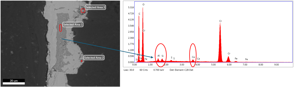
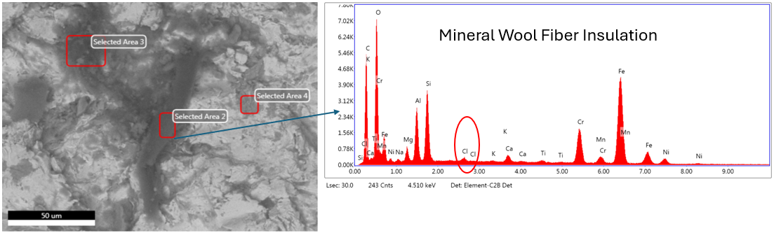
- Analyze corrosion products and deposits
- Detect inclusions, contaminants, and foreign materials
- Evaluate weld defects and heat-affected zones (HAZ)
- Characterize coatings, claddings, and diffusion layers
- Perform elemental mapping and localized chemistry analysis
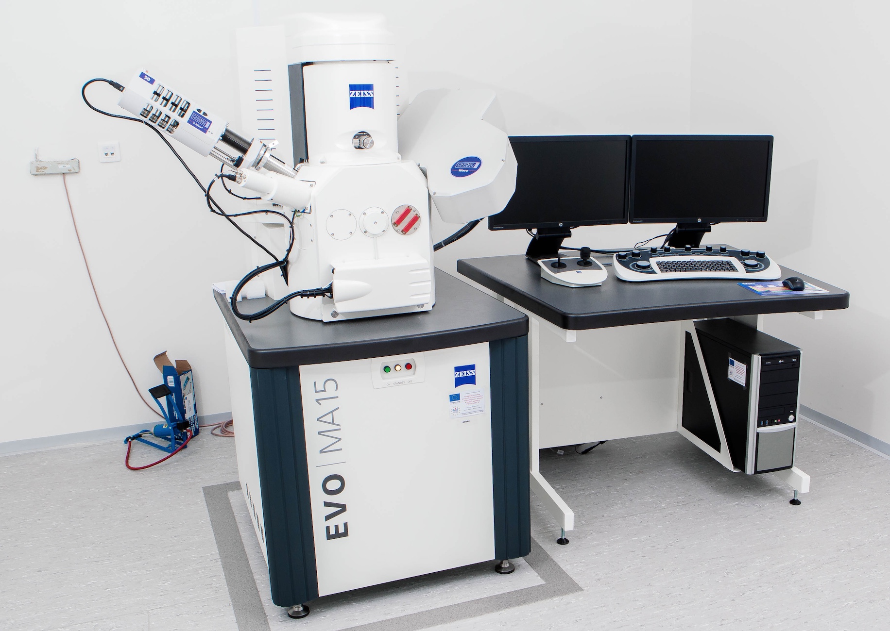
Our new variable pressure Zeiss EVO MA-15 SEM is equipped with a newly developed third generation variable pressure secondary electron detector, which allows high resolution microstructure imaging possible on non-conductive, wet or volatile samples. Typical samples we can handle include corrosion products, cloth, polymer films, plastic components, printed-circuit boards, ceramics, rocks, painted and coated metals, explanted medical devices with attached tissue, metal components encapsulated in polymer, lubricated metals and polymers. In many of these cases, evaporative or sputter coating was either undesirable or not possible. These examples show the value of eliminating sample pretreatment and the utility for performing scanning electron microscopy at variable pressures.
Pricing $350 per hour.